New Frontier Technologies in the Clean Room
IL PROGETTO
In the context of the initiative proposed by the Provincial Council of Trento (resolution No. 1412/2017) for the strengthening of the research and innovation system through the strengthening of research infrastructures of provincial relevance in terms of both the construction of new infrastructures and strengthening of existing infrastructures, Fondazione Bruno Kessler presented the project called “Key Enabling Technologies Facility in Trento” (KFT).
The project is part of the FESR 2014-2020 Operational Program: “Investment for growth and employment” objective – Axis 1 “Strengthening research, technological development and innovation” – Action 1.1.1 – “Support for infrastructure of research considered critical/crucial for regional systems “.
The FBK project envisages the upgrading of the capacity of the current Microfabrication Facility of the Center for Sensors & Devices with state-of-the-art nanofabrication equipment that will bring the Trentino area to be a reference for the national excellence of the Key Enabling Technologies. The tender documentation for the purchase of high-tech scientific equipment is available here.
The sectors that benefit from the research and innovation capabilities of FBK – S&D and which will benefit from KFT, cover application areas in all areas of the Regional S3. The enabling activity is the one related to sensors, developed at the Micro Nano Facility (MNF).
Sensors lie at the basis of scientific research, of advanced automation systems, such as those involved in the mechatronics-Industry 4.0 area (smart parts, LiDAR systems), in quality of life area (medicine and domotics), in the environment area (control of pollutants), in the agrifood area (quality control of food and soil).
KETs provide a platform that can support the provincial industrial development plans. To do this effectively it is necessary to fill the gaps by enhancing and integrating the existing resources. This project ensures coverage of all KETs, bearing in mind that with the “Pro-M Facility” the mechatronics/smart manufacturing area is already covered and, with this action, it would also increase its relevance and prototyping capability.
CONTINUING INNOVATION
In the past twenty years, Fondazione Bruno Kessler has pursued ground-breaking research, innovation and technology transfer and has achieved excellent results at the national level, as recently recognized also by the ANVUR assessment. A relevant role in this growth is played by the Micro Nano Facility (for micro-nano-manufacture), the heart of the Center for Sensors & Devices; it places the Center in a unique position at a national level for its scientific and innovation capabilities for high-tech companies, covering the entire cycle that goes from the development of basic technologies to the development of innovative marketable products.

THE CLEAN ROOM
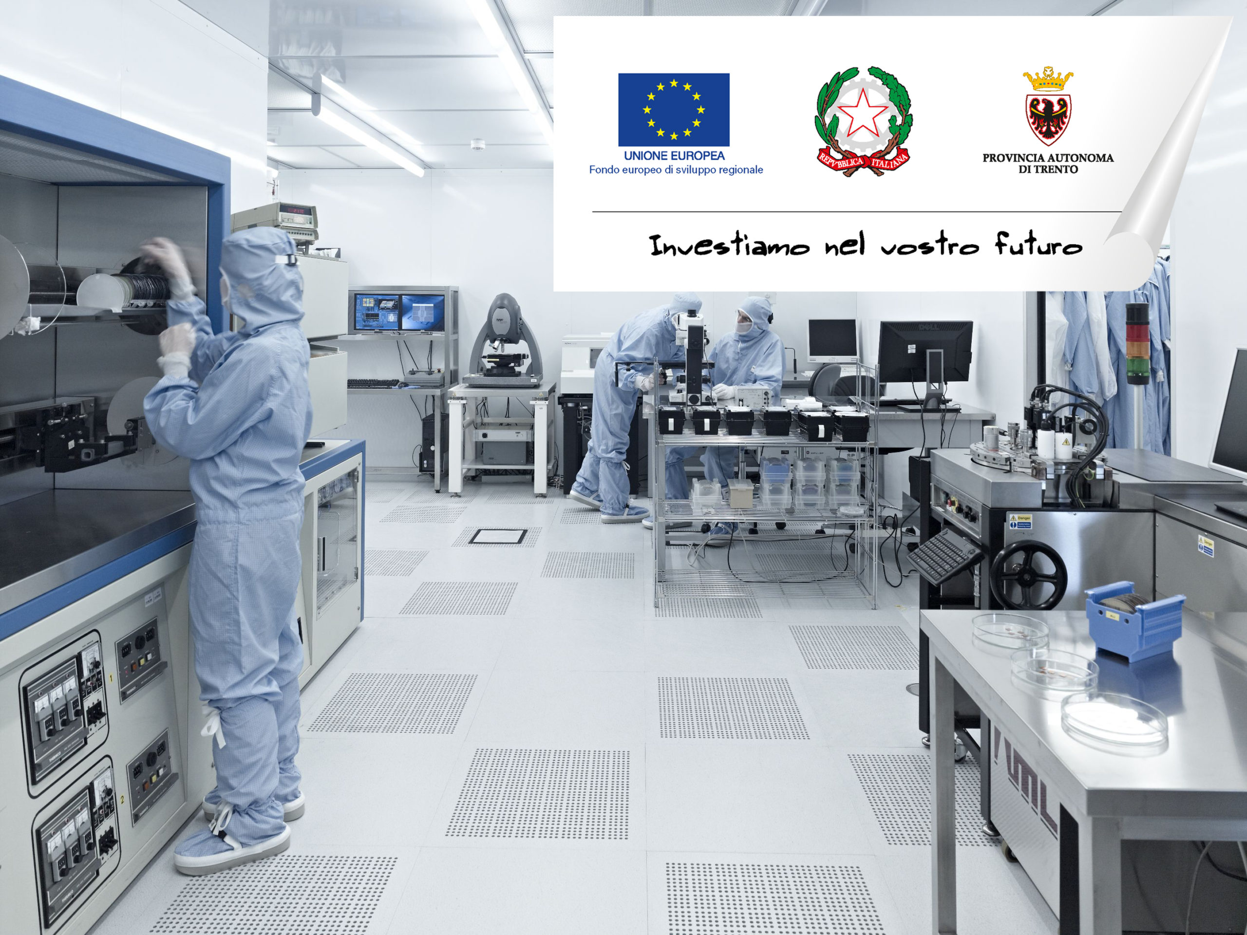
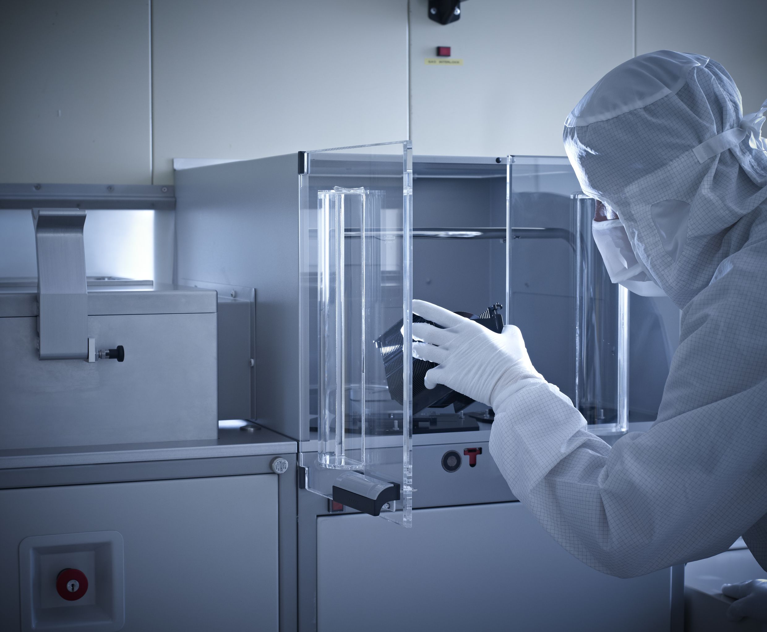
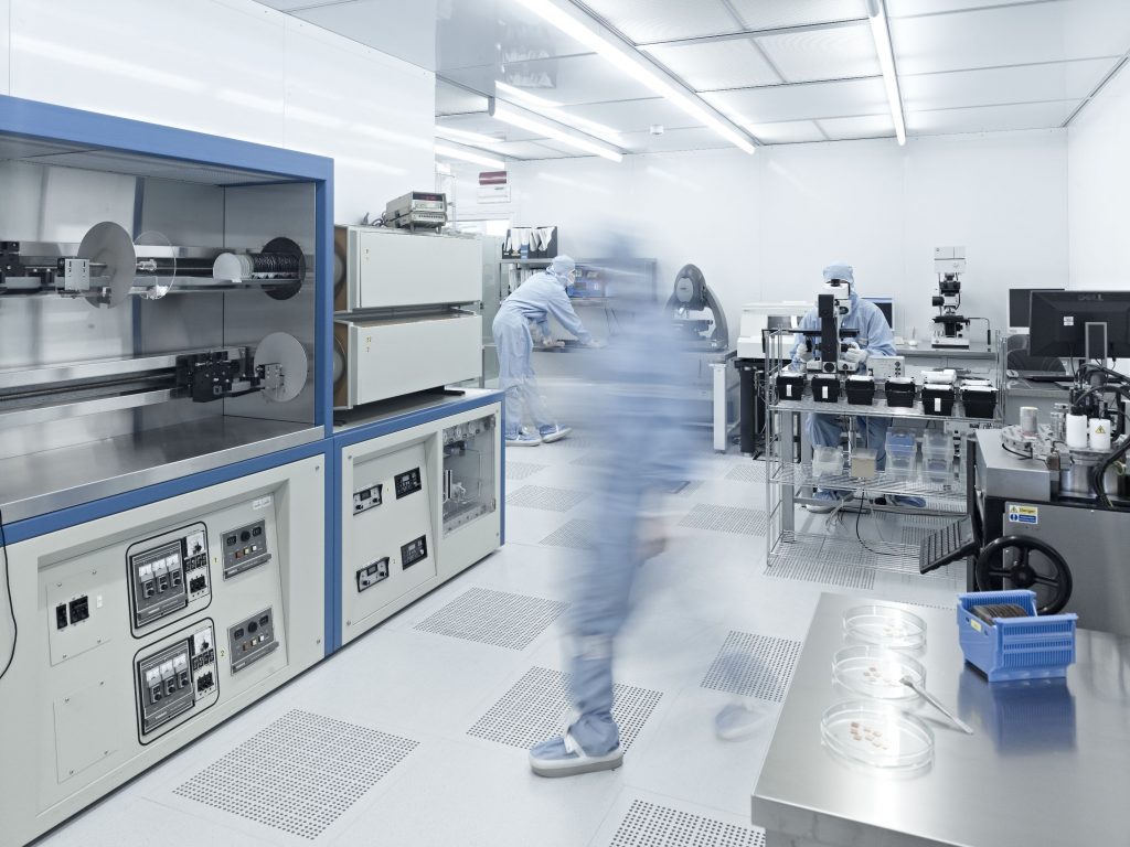
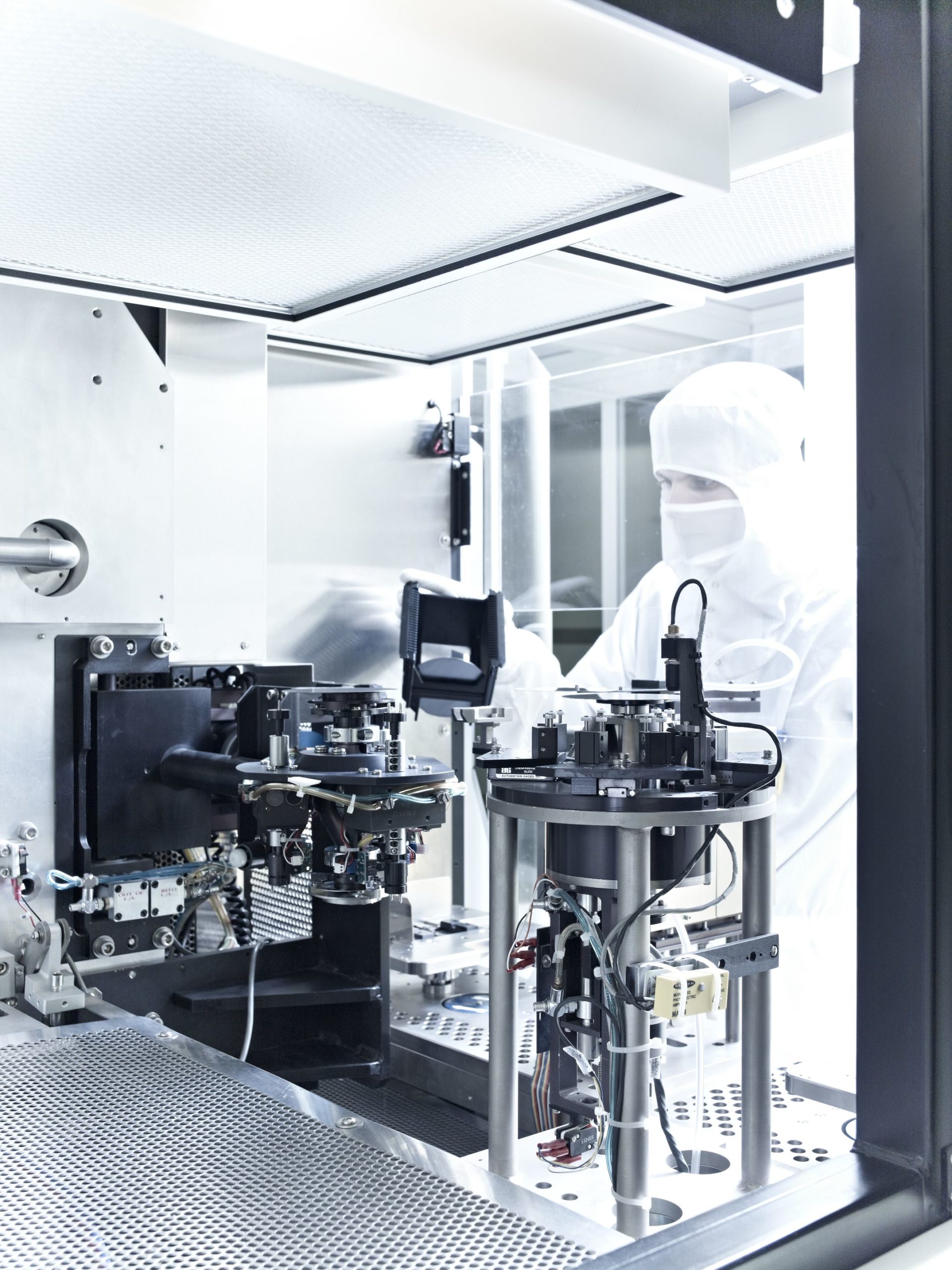
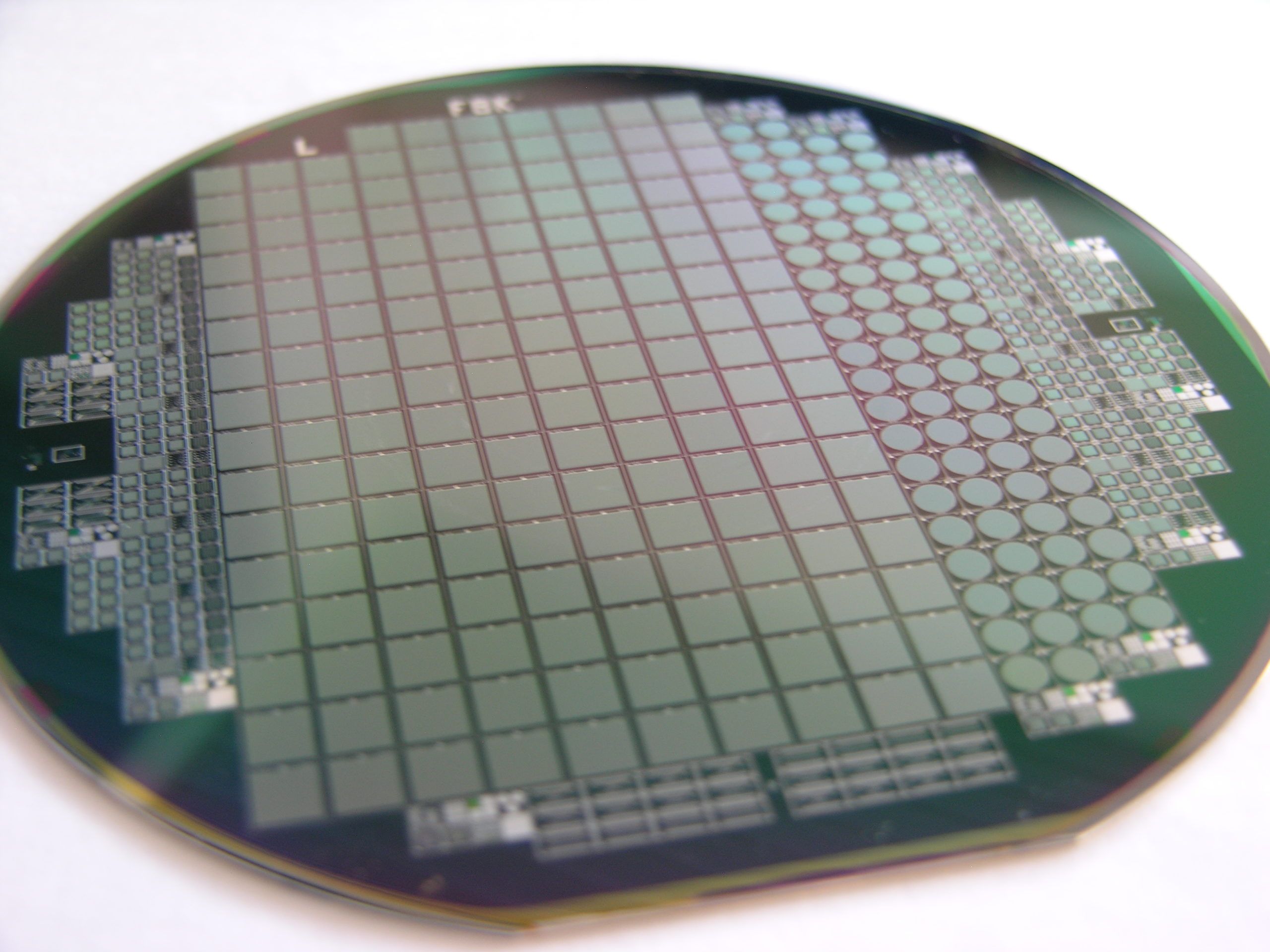
The protagonist of the project is the Clean Room: a laboratory that is cleaner than an operating room where silicon wafers are processed so that researchers can obtain radiation detectors used in fundamental physics experiments. Some of these detectors are in the CERN particle accelerator in Geneva, others are in orbit on the International Space Station.
Currently, the Clean Room occupies an area of 700 square meters and it is fully equipped to produce, starting from 15mm silicon wafers, radiation detectors and MEMS (Micro-Electro-Mechanical Systems) for the characterization of materials and micro-nano-fabrication. All this makes of it a worldwide reference point in the support of scientific research and innovation. Its beating heart is the remarkable expertise of the staff gained over the course of its long history of silicon processing.
Excellence and expertise gained over almost 30 years mean that our characterization and micro-nano-manufacturing facilities reach the highest levels. This is the place where our sensors are created:
THE RESEARCH
S&D Center has an internationally recognized scientific tradition in the development of MEMS, photonics, microelectronics and microfabrication technologies. Scientific know-how in these domains allows the development of systems and devices integrating heterogeneous technologies. The high degree of miniaturization, the integration of different functions for detection and actuation, signal processing and data transmission are the elements that characterize this approach. For several years, S&D has pursued research in the field of complex microsystems, exploring architectures of adaptive devices for a variety of application environments.
The Center’s know-how includes, among others, the following items:
- As for MEMS, the Center has dealt with a broad spectrum of technologies including RF-MEMS (RadioFrequency MEMS) for the development of innovative devices in the satellite telecommunications industry, MEMS sensors for automotive industry (braking system sensors) and space (GAIA, LISA PATHFINDER, MICROSCOPE positioning systems). In basic research, interest in the development of bolometers for applications in the study of particle physics and quantum physics.
- As far as BioMEMS are concerned, the focus is on the development of microanalysis systems for food quality control and biomedical applications. Examples include portable micro-analysis systems (lab-on-chip, point-of-care systems) based on chemical and biological sensors, microfluidic modules and minimally invasive systems for monitoring of physiological parameters (wearable sensors, smart lenses). At FBK, these systems have reached a high level of complexity and technological reliability.
- Micro-nanoelectronics (adaptive memories) and flexible electronics (thin silicon conformable sensors) are studied with a long-term perspective. Here, the combination of knowledge in the technologies for nanostructured materials and that in organic semiconductors plays a very important role.
- In the sensor and silicon technologies areas, the Center has reached levels of excellence witnessed by the presence of devices in major international experiments (e.g. ALICE, ATLAS at CERN). The Center holds leading technologies in the photon detection (SPADs, SiPM) and particles (SDD, 3D sensors).
- The Center has dealt with research in integrated photonics and nanophotonics for about 20 years. The research on silicon nanoparticles and nanofibers is important, that has led to the development of increased efficiency solar cells, the creation of new energy harvesting devices by exploiting the Seebeck effect, and the development of random number generators from quantum phenomena. Integrated photonics research has brought both scientific excellence and technology-relevant results (such as the development of an integrated optical circuit for biosensors). The center is now capable of developing optical circuits integrated with various frontier technological platforms (silicon nitride, crystalline silicon and polycrystalline diamond).
The above points testify to the lively and recognized international quality of research at S&D, which operates on topical research areas. These will benefit from a considerable impulse from access to nanotechnology guaranteed by the KFT project.
SIGNNIFICANT DATA
Funding: 8 million euros
Length: 24 months from the start date of the works
Additional documentation available here
The initiative is implemented under the FESR 2014-2020 Operational Program of the Autonomous Province of Trento thanks to financial support from the European Union – European Regional Development Fund, the Italian State and the Autonomous Province of Trento.